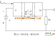
PIN光电二极管是在PN结的P型层和N型层之间夹了一层本征半导体(semiconductor ,形成P-I-N结构而得名,如下图所示:如上图所示,处于...
稳压二极管组成的基本稳压电路
稳压二极管组成的基本稳压电路图:
图1电路是一个采用稳压二极管(齐纳二极管)的简单稳压器电路。

Figure 1. Simple Zener Shunt Stabilizer Circuit Diagram
The circuit in Figure 1 is a simple voltage STabilizer circuit that employs a zener diode and a single resistor. In this circuit, the zener diode, which is the stabilizing component, is in parallel (or in shunt) with the load, which is why it is also called a shunt stabilizing circuit. The value of R must be chosen so that a 'holding current' of 2 mA will flow into the zener diode even at the lowest input voltage and maximum load current. The zener diode maintains the output voltage level by 'conducting' the excess current to ground whenever the voltage across it becomes excessive.

Figure 2. Amplified Zener Shunt Stabilizer Circuit Diagram
The circuit in Figure 2 is another shunt voltage stabilizer circuit that employs an additional NPN transistor to the simple circuit in Figure 1. In this circuit, the zener diode no longer has to conduct large currents to stabilize the output voltage. The transistor takes care of conducting the excess current whenever the current required by the load drops. This circuit is also known as the "amplified zener' shunt stabilizer.
相关文章

发表评论